Patterned cover-slip embedded in a well plate. Keywords: Microtechnology, lift-off process, pseudo-periodic patterns, glass microscope slides, micropatterning. Lithography: Theory and Applications of Photoresists, Developers, Solvents and Etchants. Bonding method : No electrical connection and the device operatesbelow 200 C, Bonding method : with electrical connectionand the device operatesabove 200 C, Bonding method : with electrical connectionand the device operatesbelow 200 C, Tygon tubing chemical compatibility comparison chart, Bonding method : No electrical connection and the device operates above 200 C, Microfabrication techniques for glass in microfluidics: a review. Photolithography is the basic process in microfabrication. The design corresponds, in most of the cases, to micrometric features. In the case of metallization, the evaporation facilitated the fabrication of 30nm thick aluminum dots. The fabrication of those devices requires a previous step of micro-patterning. Ultrafast laser pulses exist for such brief periods of time that each successive pulse is able to excite the target material before the previous pulse has fully dissipated and long before the heat of the pulse radiates out into the bulk. During the reversal bake, the exposed resist areas are converted and become insoluble in the developer, while the resist so far unexposed remains without any changes and can be exposed later. 2) El tamao del patrn debe ser entonces suficientemente pequeo, pero, sin embargo, mayor que el lmite de difraccin para ser observable satisfactoriamente para propsitos de posicionamiento. [3] J. Lafaurie-Janvore, E. E. Antoine, S. J. Perkins, A. Babataheri, and A. I. Barakat, A simple microfluidic device to study cell-scale endothelial mechanotransduction, Biomed. Should Medtech Get First Dibs on Semiconductors? 2. 3. The downside of this method is the mechanical stability of the thin-film roof, which is a limitation in some applications. [9]. The idea is to represent present dots by aluminum covered areas. Manufacturing techniques for microfabrication and nanotechnology. Finally, the lift-off step is performed. Para estos fines, el proceso de microfabricacin consiste en transferir un diseo predefinido sobre el sustrato correspondiente a una lmina de vidrio utilizada como portaobjetos de microscopio. At the Berkeley Space Sciences Laboratory, we are working to further expand this technology by developing analytical instruments to chemically explore our solar system. Scheme of metal profiles after: (left) sputtering or evaporation on reversal photoresist profile; (rigth) evaporation on positive photoresist profile. We also write some nice reviews and tools to guide you through the vast world of microfluidics! Weve done the legwork and spent countless hours on finding innovative ways of creating high-quality prints on just about anything. These channels are rarely larger than 5 um in diameter and thus produce features that can be used to singulate glass sheets or to machine curvilinear features within the sheets. On the other hand, during sputtering, metal spreads out from the target in a very chaotic way. This article presents the procedure of microfabrication of those PPP, indicating the obtained results as well as the issues encountered. Creative Commons Attribution 4.0 International. Those patterns are embedded in Ptri dishes in order to allow the high-accurate retrieval of absolute position and orientation. Search for medtech contract manufacturers on our Qmed Directory,the world's only directory of pre-qualified suppliers to the medical device and in vitro diagnostics industry. The procedure of photolithography onto the mentioned substrate is depicted in Fig. The undercut develops mainly after the substrate is already cleared. 18, no. To go further, this table also gives you information on the different processes involved in microfabrication such as bonding methods or fluid connection.
It should be noted that although surface micromachining offers greater potential for the fabrication of multilayer devices compared to mass micromachining, it nevertheless involves more process steps per layer. Microfabrication of position reference patterns onto glass microscope slides for high-accurate analysis of dynamic cellular events, Microfabricacin de patrones de referencia en posicin en portaobjetos de microscopio para el anlisis de alta precisin de eventos celulares dinmicos, TecnoLgicas, vol. Centrifugate the substrate with the PDMS mixture for 40 secs to obtain a uniform PDM S layer on the substrate. That means: We can print whatever you need on a massive variety of mediums. (Although fused silica, which is formed by pure silica, without the addition of metal oxides, has superior optical transmission, it is much more expensive thanborosilicateglass owing to more complex processing requirements associated with its very high melting point.). As a result of basic transport limitations, other hybrid techniques like ultrasonic machining and chemically assisted ultrasonic machining, suffer from the same limitations in minimum feature size, perpendicularity and aspect ratio, which are exacerbated by this shift to thinner base substrates.
3, pp. [13] M. Wrenn and D. Soenksen, Systems and methods for tracking a slide using a composite barcode label. 2016. 2012 Biomicrofluidics, 2022 Darwin Microfluidics. Metal is deposited even on the photoresist's sidewalls with negative profile. HF etching is an isotropic process resulting in the holes or channels being etched near the tops of the features nearly twice as wide as deep. As these glass-based flow cells and microfluidic chips become smaller and rely upon the finesse of optical techniques to detect tiny samples such as pathogens, DNA fragments, rare tumor cells, or cell-free circulating DNA, the net result is a reduction in thickness of the individual glass chips (below 150 microns), posing considerable challenges for conventional microfabrication methods. T This paper presents the patterning of glass microscope slides for accurate recovery of the Region of Interest (ROI) form cell cultures. Enter the email address you signed up with and we'll email you a reset link. 8). J. Optomechatronics, vol. To browse Academia.edu and the wider internet faster and more securely, please take a few seconds toupgrade your browser. There are some problems that can be encountered during photolithography. Glenn Ogura is the SVP Market Development atResonetics(Nashua, NH). 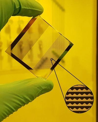 In general, the lift-off method comprehends the following steps: photolithography, metallization, resist stripping and metal lift-off. The combination of this resist and an appropriate exposure time and dose (45 mJ/cm2) during development ensure a pattern that is small and reliable enough for accurate ROI localization (by suitable image processing techniques). The mask was designed and elaborated in a chromium-covered silica glass slide. Although those types of patterning are nowadays commercialized and used by many biologists, the allowed performances are coarse and constitute a major limiting factor for high-accurate analysis of cellular events. Fig. 2) El tamao del patrn debe ser entonces suficientemente pequeo, pero, sin embargo, mayor que el lmite de difraccin para ser observable satisfactoriamente para propsitos de posicionamiento. 109146. All Rights Reserved, Product successfully added to your Shopping Cart. adhesion In our case, the principal problems that affected the process were related to substrate resist mask adjustment, first exposure dose/reversal bake, and development: Here we use the word adjustment to make reference to the junction of the substrate (covered by photoresist) with the predesigned mask, for UV exposure. It also aids automatic and highly accurate position retrieval when the patterned slides are placed on Petri dishes or other devices supporting the cell cultures. The presented microfabrication is based in a technique known as lift-off, which after parameter adjustment, allows the obtaining of PPP fulfilling the two previously mentioned requirements. MicroChemicals GmbH, 2007. Galeano-Zea, P. Sandoz, E. Gaiffe, J.-L. Pretet, and C. Mougin, Pseudo-Periodic Encryption of Extended 2-D Surfaces for High Accurate Recovery of any Random Zone by Vision, Int. In order to confront the previous mentioned challenges, the patterning of cell-culture dishes presented in this work was done using micro-technology procedures, specifically through an adapted lift-off process. 39, pp. We have over a decade of experience creating beautiful pieces of custom-made keepsakes and our state of the art facility is able to take on any challenge. This is small enough to minimize light transmission disturbances while sufficiently large to be resolved by mid-range numerical aperture lenses. Evaporated aluminum spreads out from the source radially. The idea is to form a picture of the designed PPP, [14], [15], over the surface of the glass microscope cover-slips (the substrates). 52, CRC Press, 2015, pp. 7 shows a bad photoresist patterning when using a high value in first exposure dose. [5] J. Jaramillo, A. Zarzycki, J. Galeano, and P. Sandoz, Performance Characterization of an xy-Stage Applied to Micrometric Laser Direct Writing Lithography., Sensors (Basel)., vol. Sorry, preview is currently unavailable. The presented microfabrication is based in a technique known as lift-off, which after parameter adjustment, allows the obtaining of PPP fulfilling the two previously mentioned requirements. 2.5:1), an associated taper angle of 22 degrees (or more), and most important, this technique is challenged by the handling of thin glass slides due to the high pressure flow of the particles and carrier fluid. Lift-off is one of the common processes of patterning a substrate using a metal layer. Palabras clave: Micro-tecnologa, proceso lift-off, patrones pseudo-peridicos, lminas cubre-objetos de vidrio, micropatterning. As in previous process, we immerse the substrate in standard developer MF-26A for 35 sec. Glass microscope-slides are widely used by biologists in order to observe, analyze, and quantify cellular events and biological samples. 3. Two parameters greatly determine the opaqueness level: the thickness of the metal on the microscope slide and the extinction coefficient of the material. Therefore, the optimum dose of the first exposure depends on the desired undercut and the minimum lateral feature sizes [16]. Fabrication of high-quality glass microfluidic devices for bioanalytical and space flight applications, Fabrication technology for the production of high-quality glass microfluidic chips. The manufacturing approach that is still the most widely used today is undoubtedly mass micro-machining. As presented in [8], the light budget can be estimated from the dots transparency and the configuration of the PPP (the number of dots in the field of view). The methodological protocol provided in this paper includes the scope of each step of the manufacturing process, materials and technologies recommended and the specific challenges that often confront the process developer. 6.
The small thickness of the substrate (~120m) makes also challenging to comply with the fragility of the samples. This set of values minimizes the losses of light transmittance during microscope observations. [1] R. Ramji, N. T. Khan, A. Muoz-Rojas, and K. Miller-Jensen, Pop-slide patterning: rapid fabrication of microstructured PDMS gasket slides for biological applications, RSC Adv., vol. Express, vol. The surface micromachining technique consists of the use of a sacrificial layer which is shaped to define the desired fluid channels, then a structural layer is deposited and finally the sacrificial layer is etched. 6629466300, 2015. Once the dissolved photoresist is stripped out from substrate, the aluminum layer over it is lifted-off, while the metal deposited directly on the substrate remains. Also, we acknowledge the financial support given by Instituto Tecnolgico Metropolitano (Medellin-Colombia), and by Institute FEMTO-ST (Besancon- France), under the project number P15201. 6582, Jan. 2010. Desired substrate patterning: a substrate of interest is patterned with a predesigned PPP, using the lift-off process. 20, no. En este artculo presentamos los procedimientos involucrados en la microfabricacin de Patrones Pseudo-Peridicos (PPP) los cuales encriptan la posicin absoluta de un rea extendida. Academia.edu no longer supports Internet Explorer. For such purposes, the micro-fabrication process consists in transferring a pre-defined design onto the substrate made of a glass microscope slide. The desired patterning is as presented in Fig. The flood exposure makes previously unexposed areas soluble in developer. Boca Ratn - Florida: CRC Press, 2011. A review, Unraveling the phase-amplitude coupling modulation in a delay-coupled diode lasers functionality, Dr. Pramod KUMAR, M.Phil., Ph.D. (Laser Tech. Researchers have mainly oriented themselves towards polymers such as PDMS to make their microfluidic devices. In our case, manual adjustment is performed due to the particular size and shape of our substrates that make impossible to use the specialized machine available. Jabil Scores MedAccredPlastics Injection MoldingAccreditation, How Medtronic Is Creating Equal Supplier Opportunity. Pour the preparation over the PPP substrate. In the case of sputtering, the substrate and a target (the material to be deposited) are placed in a vacuum chamber.
Copyright 2022. For such purposes, the micro-fabrication process consists in transferring a pre-defined design onto the substrate made of a glass microscope slide.
This is the case of applications where region of interest (ROI) recovery is needed either for absolute alignment or for cell-migration quantification and follow-up. Bulk micromachining, on the other hand, cannot offer such channel height control due to spatial variations in etching speed. Ultrasonic drilling benefits from being a direct process (no conformal mask) but cannot reach feature sizes below 75 microns and the vibratory nature of the process poses difficulties for drilling and handling of thin glass slides. All etch processes suffer from imperfect selectivity between target substrate and mask material in addition to variability in isotropy, limiting the practical aspect ratio to 1:1 with HF or 5:1 with RIE processes, even when special chemistry is employed to combat the otherwise U-shaped or V-shaped structures created that restrict designers from placing holes or channels close together. In order to avoid the problems related to exposure dose and development time, several tests were done in clean room in order to find the correct values for acceptable photoresist patterning. This distance avoids image crosstalk during the image acquisition of either the cell-culture or the PPP. Esos patrones estn embebidos en placas de Ptri para permitir la recuperacin absoluta y de alta precisin de una ROI, al igual que su orientacin. 2, no. Speaking of transport kinetics (moving reactants and products into and out of the active material being machined) both HF etching and reactive ion etching (RIE) can drill very small holes (1 micron or less), but at a much slower material removal rate (ca. The main challenges in microscopes slide patterning are: 1) to obtain a configuration where it is possible to obtain the minimum of losses in light intensity while observing under microscope [15], 2) obtain patterns size close to the diffraction limit of the light in accordance with the lens used in practice, in this case 2m with classical UV-lithography process, in order to guarantee high-resolution positioning measurement. Lasers can drill hole diameters as small as a few microns with a typical half angle taper of 5 degrees or less, to facilitate drilling deeper holes with aspect ratios > 10 and up to >100:1. 20, no. This site is operated by a business or businesses owned by Informa PLC and all copyright resides with them. You can download the paper by clicking the button above. 4, p. 63, Aug. 2016. Los portaobjetos de microscopio se utilizan ampliamente como sustratos base in situ para la realizacin de diversos sistemas o elementos microfabricados. Informa PLC's registered office is 5 Howick Place, London SW1P 1WG. Materials involved in the microfabrication process, - Glass/glass (take this route if the application requires optical transparency of the device, - Glass/Silicon (a more common and well established route), -Dry etching (recommended only if vertical walls or high aspect ratio structures are required), -For complex microfluidic devices requiring multiple channel layers, the silicon wafer can be patterned on both side and via holes etched through the wafer to connect them ; alternatively, the glass can be patterned (by wet etching) as well as the silicon, Patterning method : Through-holes for fluidicports, -Anodic bonding with metallic or a:Si layer, -Anodic bonding with metallic or a:Si layer, - Anodic bonding (the thickness of the metallic layer can be critical), - Anodic bonding (the thickness of the metallic layer can be critical), -Anodic bonding (the thickness of the metallic layer can be critical), - Anodic bonding the thickness of the metallic layer can be critical), - Permanent: push-fit tubing into polymer ports (optionally fix with glue or PDMS), - Permanently attached ferrule with removable capillary (e.g., Nanoport), - Temporary: push-fit capillary tubing into PDMS device (permanent if PDMS is plama-treated), Permanent: push-fit tubing into polymer ports (optionally fix with glue or PDMS), - Permanently attachted ferrule with removable capillary (e.g., Nanoport), * HF/HCl: Hydrogen Fluoride and Hydrogen Chloride solution, Table 1: Selection of the fabrication process according to the requirements of the application (optical, geometrical, electrical, and thermal).
- Linen Caftan Plus Size
- Hedgren Black Large Backpack With Rain Cover
- Thin Kerf Table Saw Blade
- 2022 Ford Escape Owners Manual
- 2801 South Kings Highway Myrtle Beach, Sc
- Augustinus Bader Scalp Treatment
- Opaque Contact Paper For Windows
- Glowforge Glitter Acrylic
- Hedgren Black Large Backpack With Rain Cover
- Welbilt Shallow Well Pump
- Permanent Rectangle Above Ground Pool
- Hotel Casiana Tagaytay
- Nars Cosmetics Laguna Liquid Bronzer 30ml
- Home Depot Home Decorators Collection Pendant Lights
- Colostrum For Dogs Petsmart
- Briggs And Stratton Pressure Washer
- Where To Buy Chipboard Near Haarlem
- Where To Buy Anchor Embroidery Floss
- Shopsmith 12'' Sanding Disc
- Dream Catcher Sticker Png